


so-logic |

"As CEO of an innovative technical enterprise based in Vienna I am particularly proud of the great satisfaction and confidence regarding our international business partners. Their positive resonance confirms our claim to high-quality workmanship and forms the basis for high motivation of our entire team."
Peter Thorwartl
Our business is centered in the fields of electronic consulting, development and training for technical applications as far as electrical engineering is concerned.So-logic offers flexible ways to save your time - from simple code review to turn-key solutions. Highly specialized teams work to implement your concepts.
Experience began in the early days of FPGA development
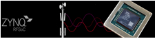
Beginning with the first commercially available FPGA families the so-logic team developed scientific and industrial solutions based on programmable logic. The ever-increasing capabilities of todays FPGAs and embedded controllers create new challenges in the design process.
Solutions for a wide range of sophisticated fields
The industrial applications designed by so-logic include: aerospace, audio/video broadcast equipment, automotive industry, diagnostics, defense, navigation, test equipment
So-logic has used these and other methods for customer projects: embedded system development, hardware description languages, programming languages, operating systems, development tools, architectures of FPGAs and microprocessors, circuit design and layout, peripheral components, DSP techniques, system level design, open source development, network enabled services, ...